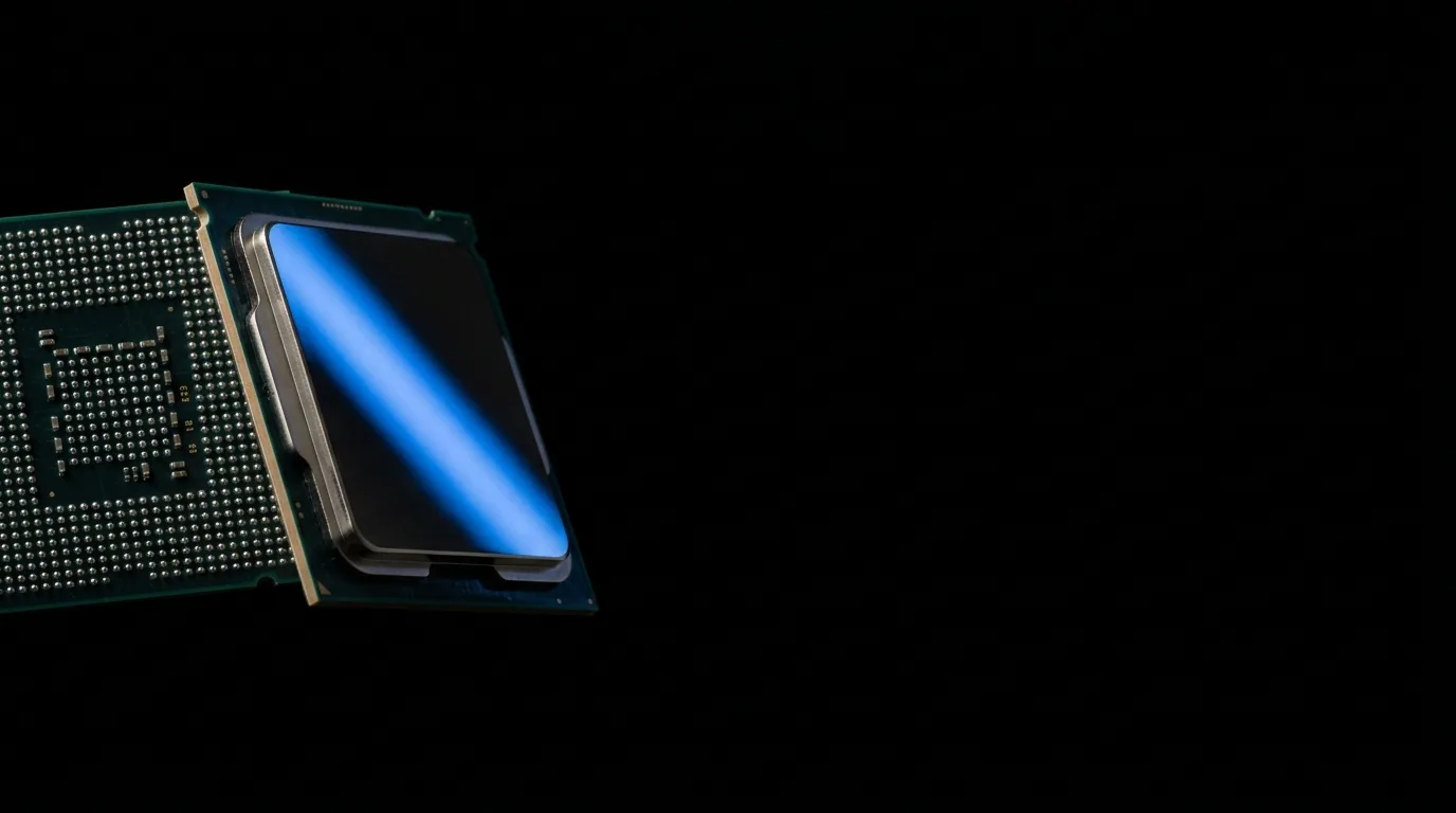
How TSMC Allocates N3E Wafers - And Why Apple Eats the Supply Before NVIDIA Gets a Wafer
The TSMC 3nm GPU supply constraints problem starts before NVIDIA's engineers write a single line of firmware. TSMC's N3E process - the node powering the Rubin R100 - runs at roughly 120,000 wafers per month at full capacity. Apple books somewhere between 60 and 70% of that for the M4 and A18 chip families. NVIDIA, AMD, Qualcomm, and the rest compete for what remains.
This is not a new dynamic. Apple has anchored TSMC's leading-edge capacity since the A9 in 2015. TSMC builds fabs around Apple's annual iPhone cycle, and NVIDIA's AI GPU ramps happen to compete with that same silicon. When iPhone season peaks in Q3-Q4 each year, TSMC's allocation pressure maxes out. NVIDIA's GB200 ramp in late 2024 ran directly into Apple's A18 production window. The Rubin R100 will hit the same wall in late 2026.
The wafer allocation problem compounds because leading-edge fabs take 3-4 years and $15-20B to build. TSMC's Fab 21 in Arizona (N3/N2 capable) will not reach meaningful production capacity until 2027-2028 at earliest. So for the entire Rubin launch window, TSMC's N3E output is essentially fixed - a zero-sum competition between the world's most profitable consumer electronics company and the world's most valuable semiconductor company.
3 Supply Chain Failures That Caused Blackwell's 36-52 Week Lead Times - and Will Repeat With Rubin
B200 lead times hit 36-52 weeks because three independent supply chains all constrained simultaneously. The process node (TSMC N4P) was fine. What collapsed was CoWoS advanced packaging capacity, HBM3e supply from SK Hynix, and the substrate supply for the NVLink interconnect boards. Any single one of those constraints would have stretched lead times. All three at once made B200 the hardest GPU to procure since the H100 launch.
CoWoS-L (Chip on Wafer on Substrate, Local variant) is how NVIDIA bonds the GPU die to the HBM memory stacks without a traditional silicon interposer. In early 2024, TSMC's CoWoS-L throughput was roughly 6,000-8,000 substrates per month - a trivially small number when a single GB200 NVL72 rack requires 72 packaged GPUs. That single bottleneck was responsible for most of the availability story. The hyperscalers knew it. NVIDIA knew it. It still took nine months from announcement to any meaningful non-hyperscaler allocation.
The HBM3e story is the more instructive one for Rubin buyers. SK Hynix held roughly 60% of HBM3e supply at B200 launch. Samsung was 12-18 months behind on qualification. Micron was in pilot production at best. When your most differentiated component comes from a single supplier, lead time is a function of that supplier's capacity ramp - not your purchasing power. The R100 faces an identical structure with HBM4, except SK Hynix's lead over Samsung on HBM4 is larger than it was on HBM3e.
Rubin R100 on N3E - Why a Dual-Die 336B Transistor Package Makes Shortages Structural
The Rubin R100 is a dual-die design: two GR100 chiplets bonded via NVLink interconnect on a single package, totaling 336 billion transistors. That is not an incremental change from Blackwell's single-die approach - it is a packaging complexity step-change that compounds every supply chain constraint. Each additional die-to-die connection on a CoWoS substrate adds yield risk. More yield risk means more silicon consumed per working unit, which means the effective production rate is lower than raw wafer starts suggest.
Packaging yield for dual-die designs at N3E dimensions is currently estimated at 60-70% at mature production. But R100 is not a mature design - it is a new architecture at a process node that only entered high-volume production in 2023. Early yield on first-generation dual-die packages at leading-edge nodes historically runs 15-20 percentage points below mature yield. Call it 45-55% in the first six months of production. At 50% yield, NVIDIA needs twice as many CoWoS substrates - and twice as many HBM4 stacks - to produce the same number of working R100 GPUs.
This is the part GPU roadmap slides never show. NVIDIA can truthfully say R100 is sampling in Q4 2026 while the actual delivery timeline to a mid-market buyer remains 14-18 months away. 'Sampling' means 100-500 units to Google, Microsoft, Amazon, and Meta labs. 'Volume' means 50,000+ units flowing through the broader market. Those are categorically different milestones, and the gap between them is measured in manufacturing yield curves, not product schedules.
HBM4 Supply Chain - How SK Hynix, Samsung, and Micron Capacity Actually Gates Rubin Production
HBM4 is what makes R100 faster than Blackwell, and HBM4 supply is what makes R100 scarce. SK Hynix is targeting 1 TB/s bandwidth per stack for HBM4 - more than double HBM3e's roughly 460 GB/s - using a 16-hi stacking architecture that is fundamentally harder to manufacture than HBM3e's 12-hi design. Each additional layer in the stack adds micro-bump bonding steps and thermal management complexity. Early yield estimates on SK Hynix's 16-hi HBM4 prototypes have consistently shown 40-60% pass rates in internal roadmap presentations.
Samsung's HBM4 roadmap has slipped multiple times. The company that was expected to qualify HBM4 in early 2026 is now tracking toward volume production in 2027. Micron is further behind - still working through HBM3e volume ramp as of mid-2025, with HBM4 samples not expected until late 2026. The practical implication: SK Hynix will supply 70-80% of all HBM4 for R100 launch units, giving them effective control over the entire Rubin production timeline.
Here is the math that matters: a single R100 GPU requires 6-8 HBM4 stacks. At 50% early yield on those stacks, the supply chain needs to start with 12-16 stacks to deliver one working GPU memory configuration. That doubles the effective HBM4 cost per shipped unit and creates a hard ceiling on R100 production ramp that is completely independent of how many N3E wafers TSMC fabricates. This is why the AI GPU supply chain is not a single bottleneck - it is a series of bottlenecks that stack.
| Factor | B200 (Blackwell) | R100 (Rubin est.) |
|---|---|---|
| Process Node | TSMC N4P | TSMC N3E |
| Die Configuration | Single die | Dual-die GR100 |
| Transistors | 208B | 336B |
| Memory Type | HBM3e | HBM4 |
| Primary Memory Supplier | SK Hynix (60%) | SK Hynix (75%+ est.) |
| CoWoS Yield (early prod.) | ~65% | ~50% est. |
| Hyperscaler Sampling | Q2 2024 | Q4 2026 (confirmed) |
| Broad Market Volume | Q1-Q2 2025 | Q3-Q4 2027 est. |
| Expected Lead Time | 36-52 weeks | 52-72+ weeks est. |
When Will Rubin Actually Ship? A Realistic Timeline - Not the Slide Deck Version
NVIDIA confirmed R100 sampling to hyperscalers in Q4 2026. Google, Microsoft, Amazon, and Meta will get early units. Everyone else waits. The historical pattern from Blackwell is the most accurate guide available: B200 sampled to hyperscalers in Q2 2024, and meaningful allocations reached neocloud providers like CoreWeave and Lambda in Q1-Q2 2025. Nine to twelve months between hyperscaler sampling and non-hyperscaler availability. That gap exists because hyperscalers absorb 80-90% of initial production.
Apply that same gap to R100: hyperscaler sampling in Q4 2026 means neocloud availability in Q3-Q4 2027 at the earliest - and that assumes no additional supply chain setbacks. Volume availability through secondary markets and broker networks, where early-allocation holders sell excess capacity from test deployments, likely arrives in Q1-Q2 2028 for buyers without a direct NVIDIA relationship or hyperscaler contract. That is not pessimism. It is arithmetic.
For context: NVIDIA announced both Blackwell and Rubin at GTC in March 2024. Eighteen months after that announcement, B200 availability outside hyperscaler channels remained constrained. The teams that understood the supply math went and locked in H200 contracts in Q2-Q3 2024 instead of waiting. They had production AI infrastructure running while competitors sat on waitlists. The buyers making that same correct decision for 2027 are not waiting for Rubin sampling news - they are securing Blackwell Ultra capacity now.
Navigating TSMC 3nm GPU Supply Constraints: 3 Decisions AI Teams Must Make Before Rubin Ships
First: if your 2027 infrastructure plan depends on R100, start the provider conversation now - not after the launch event. Priority allocation agreements for next-generation GPUs require lead time themselves. The teams that had B200 in Q2 2025 made their reservation calls in Q3-Q4 2024. Some of those agreements allow substitution to Blackwell Ultra (B300) during the interim, which gives you production capacity while R100 supply ramps. A B300 cluster running your workload in Q1 2027 is worth more than a paper R100 reservation.
Second: build your Blackwell position now while supply is available. H200 spot rates have moderated to $3-4/hr on broker networks. B200 and B300 are increasingly accessible as production ramps through 2026. H100 capacity trades under $1.50/hr on secondary markets - pricing that was unthinkable 18 months ago. The AI GPU supply chain TSMC capacity constraints that defined 2024 pricing are softening on current-generation silicon. That window will close again when Rubin demand materializes and Blackwell demand does not disappear.
Third: understand that broker networks surface capacity the official channel does not show. When a hyperscaler receives 500 R100 units for a test deployment and only needs 200 in the first quarter, those other 300 units flow through secondary channels. That is exactly how ClusterBid sources early-generation allocations - the same dynamic that created the only realistic path to B200 capacity outside of AWS and Azure in late 2024. Check the inventory at clusterbid.com/inventory before concluding that the supply chain has nothing for you. The flexibility is there if you know where to look.