The Rubin Platform
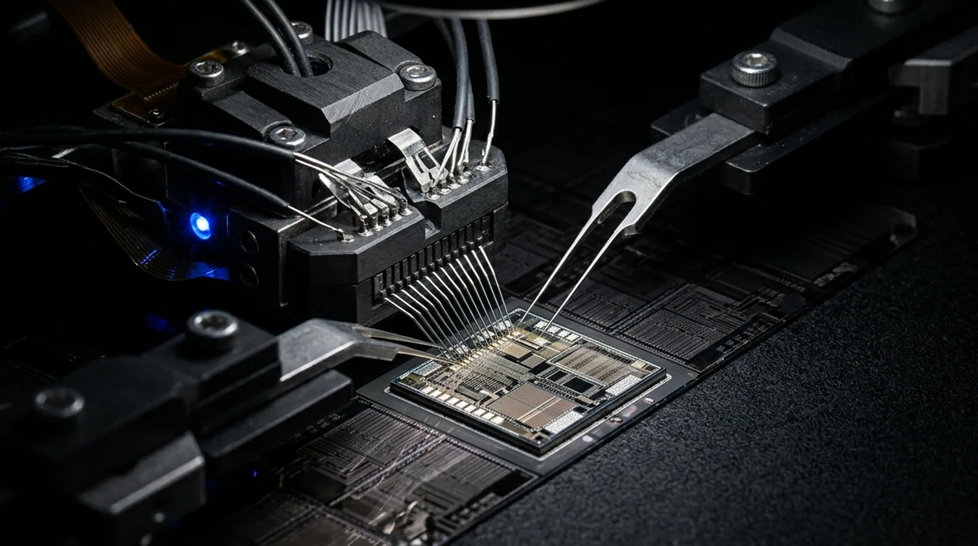
NVIDIA's Rubin architecture, named after astronomer Vera Rubin, represents the largest architectural leap since the Volta-to-Turing transition. The platform is built around three new silicon components: the R100 GPU, the Vera CPU, and the sixth-generation NVLink switch. Unlike Blackwell, which was a GPU-only refresh, Rubin introduces a full system architecture with a custom ARM-based CPU complex.
The R100 GPU is fabricated on TSMC's N3P process, moving away from the N4P used for Blackwell. This node shrink enables approximately 1.7x the transistor count at roughly 320 billion transistors per GPU. The die is split into a multi-chiplet design with compute die, memory die, and I/O die on a shared interposer, similar to but more aggressive than Blackwell's design.
Vera CPU and the Grace Successor
Vera is NVIDIA's second-generation custom ARM-based CPU, replacing Grace in the Grace Hopper and Grace Blackwell designs. Vera features 88 ARMv9 cores with SVE2 support, up from 72 Neoverse V2 cores in Grace. The memory subsystem supports eight-channel LPDDR5x at 8,533 MT/s, delivering approximately 546 GB/s of memory bandwidth to the CPU.
For AI teams, the Vera CPU matters most in two scenarios: data preprocessing pipelines that run on the CPU before GPU training, and inference deployments with disaggregated prefill where the CPU handles scheduling and tokenization at extreme scale. The Vera-to-R100 interconnect uses NVLink 6 at 256 GB/s, double the Grace-to-Hopper bandwidth.
R100 GPU Core Architecture
The R100 GPU introduces fourth-generation Tensor Cores with native support for NVFP4 and NVFP2 precisions. NVFP4 delivers 2x the FLOPs of Blackwell's FP4 implementation by using a shared-exponent block format. For transformer inference, early NVIDIA benchmarks suggest up to 1.8x throughput improvement over B300 at equivalent model quality.
CUDA core count per GPC has increased from 128 in Blackwell to 192 in Rubin, driven by the denser N3P process. The R100 contains 12 GPCs versus the B300's 8, bringing the total CUDA core count to approximately 26,112 FP32 cores per GPU. The Tensor Core array scales proportionally to 1,632 fourth-gen Tensor Cores.
| Specification | B300 NVL | R100 NVL |
|---|---|---|
| Process Node | TSMC N4P | TSMC N3P |
| Transistors | 208B | ~320B |
| Tensor Cores (Gen) | 3rd Gen | 4th Gen |
| NVFP4 TFLOPS | ~10 PFLOPS | ~18 PFLOPS |
| HBM Type | HBM3e | HBM4 |
| HBM Capacity | 288 GB | 384 GB |
| Memory Bandwidth | 8 TB/s | 12 TB/s |
| TDP | 1,000W | 1,800W |
NVLink 6 and NVL144 Scale-Out
NVLink 6 is the headline interconnect feature of the Rubin generation. Per-GPU bidirectional bandwidth reaches 2.3 TB/s, a 28% increase over NVLink 5's 1.8 TB/s. The physical layer moves to 224 Gbps PAM4 signaling, requiring shorter PCB traces and active retimers on the NVLink switch board.
The NVL144 rack configuration connects 144 R100 GPUs through 18 NVLink 6 switches in a 3-level fat tree. Aggregate bisection bandwidth across the rack reaches 165 TB/s, compared to 130 TB/s for the NVL72 rack with B300. For training trillion-parameter models, this reduces all-reduce time by approximately 35% versus the B300 NVL72 configuration.
Rubin also introduces NVLink Domain Expansion, allowing up to 576 GPUs in a single NVLink domain by chaining four NVL144 racks. This eliminates the need for InfiniBand or Ethernet for intra-domain communication, simplifying the networking stack for clusters of this size.
HBM4 Memory Subsystem
The R100 is the first GPU to ship with HBM4 memory, built to the JEDEC HBM4 standard. Each stack delivers 2 TB/s of bandwidth at a 6.4 Gbps data rate across 16 channels per stack. The R100 pairs with six HBM4 stacks for 384 GB of capacity and 12 TB/s of aggregate bandwidth.
HBM4 moves from a 1,024-bit interface per stack to a 2,048-bit interface by using a 32-die stack with through-silicon vias on a 2.5D interposer. This doubles the number of TSVs compared to HBM3e, increasing manufacturing complexity. Yield rates on early HBM4 production runs are reportedly below 60%, which will constrain R100 availability through at least Q2 2027.
Power and Cooling Reality
The R100's 1,800W TDP per GPU represents a 80% increase over the B300's 1,000W. An NVL144 rack of 144 R100 GPUs draws approximately 260 kW just for the GPUs, plus another 40 kW for the Vera CPUs, NVLink switches, and system components. Total rack power approaches 300 kW, up from approximately 140 kW for a B300 NVL72 rack.
Air cooling is impossible at these densities. Every Rubin deployment requires direct-to-chip liquid cooling with a minimum flow rate of 2.5 L/min per GPU. Data centers must support 120 kW+ per rack with coolant supply temperatures at 35-45 degrees C. Only approximately 15% of existing GPU data centers meet these specifications, meaning Rubin deployment will require new construction or major retrofits at most facilities.
What AI Teams Should Plan For
Rubin availability for cloud rental is projected for Q3 2027 at the earliest, with volume availability in Q1 2028. Teams planning 18-month infrastructure budgets should assume they will be on Blackwell or Hopper hardware through at least mid-2027. Rubin economics will initially command a premium: early pricing estimates suggest $8-$12/GPU/hr for spot instances, roughly 2x the B300 rate.
For teams that can wait, the R100's FP4 throughput and HBM4 capacity will deliver roughly 2.5-3x cost-per-token improvement over B300 for inference-heavy workloads. Training gains are more modest at 1.5-1.8x improvement, driven primarily by the larger NVLink domain and higher memory bandwidth. Teams should reserve Rubin capacity now only if they have a firm timeline for trillion-parameter model training in late 2027.